Semiconductor Jobs
Finding the people that are innovating the future
With the rise of India as a semiconductor talent powerhouse, we embrace the mission of equipping organizations with the brightest minds in semiconductor technology, from VLSI design to advanced chip manufacturing and packaging. Our approach is deeply rooted in understanding your company’s goals and delivering skilled professionals ready to lead the industry forward.
Whether you’re building cutting-edge fabs or driving next-gen innovations, our specialized expertise and global connections ensure that every hire makes an impact. Together, we’re shaping a future where India fuels the global semiconductor revolution, one mind at a time.


Our approach
Headhunters
You want the best talent, not just the best available. We leverage our vast network and extensive database, to proactively source and connect you with exceptional passive candidates.
Specialists
We speak your language and are deeply embedded in the electronics industry, possessing a nuanced understanding of the challenges and talent landscape.
Technology
Find Specialized Talent for the Semiconductor Industry – From Cleanroom Operators to Advanced Chip Designers. Click to Explore Skilled Candidates in Every Niche!
Cleanroom Manufacturing Technician
Skills Offered
Expertise in wafer handling, maintaining high cleanliness levels.
Education/Certifications Required
Diploma/B.Tech (Electronics/Mechanical); Cleanroom Certification.
Why Critical
Ensures defect-free production crucial for yield improvement.
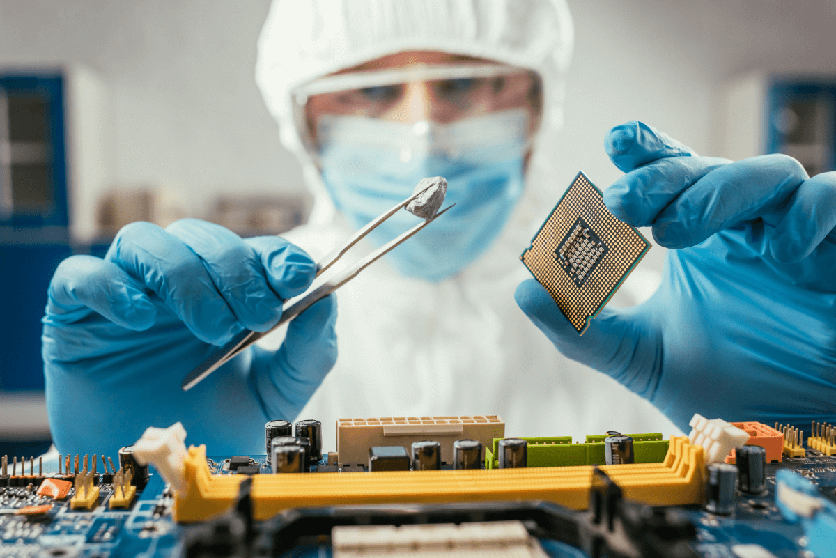
Packaging and Assembly Operators
Skills Offered
Knowledge of IC packaging, wire bonding, precision defect inspection.
Education/Certifications Required
ITI/Diploma; ISO Inspection Certification (Optional).
Why Critical
Protects and integrates semiconductor devices in the final manufacturing stage.
Process Engineers
Skills Offered
Optimization of processes like deposition/etching for production efficiency.
Education/Certifications Required
B.Tech/M.Tech (Materials Science, Semiconductor Physics); Process Certification (from SEMI or equivalent).
Why Critical
Drives productivity at fabs through yield enhancement.
Design Engineers
Skills Offered
Circuit layout design and VLSI expertise.
Education/Certifications Required
B.Tech/M.Tech (ECE, VLSI); Software Certification (Synopsys, Mentor Graphics).
Why Critical
Central to chip innovation and developing AI/IoT circuits for future technologies.
Test Engineers
Skills Offered
Chip diagnostics, error troubleshooting using automated testing equipment.
Education/Certifications Required
Diploma/B.Tech (Electronics); Certification in ATE (Automatic Test Equipment, e.g., Advantest tools).
Why Critical
Ensures chip quality by identifying errors before mass production.
Equipment Maintenance Technicians
Skills Offered
Maintenance of OEM tools like ASML wafer steppers, Lam plasma etchers.
Education/Certifications Required
ITI/Diploma; Hands-on OEM Certifications (ASML, Lam, Applied Materials).
Why Critical
Supports smooth fab operation and reduces equipment downtime.
Facilities Engineers
Skills Offered
HVAC systems management, ultrapure water treatment, chemical delivery.
Education/Certifications Required
B.Tech/Diploma (Mechanical/Environmental); Safety/ISO Certifications.
Why Critical
Critical for sustaining unswerving fab infrastructure for semiconductor manufacturing.
IT Support Engineers
Skills Offered
Expertise in MES (Manufacturing Execution Systems), cybersecurity, automated systems.
Education/Certifications Required
B.Tech (IT/CS); MES Certifications (example Siemens MES or FabTech MES Certifications).
Why Critical
Semiconductor manufacturing depends heavily on automated processes and IT-driven workflows.
Quality Control Specialists
Skills Offered
Proficient in QA tools like SEM (Scanning Electron Microscopes), defect spotting.
Education/Certifications Required
Diploma/B.Tech; Advanced Quality Certification (e.g., ISO-certified QA standards).
Why Critical
Maintains high product quality and minimize failures in global supply chains.
Failure Analysis Engineer
Skills Offered
Expertise in post-production testing and debugging physical-based chip challenges using systems like TEM (Transmission Electron Microscopy).
Education/Certifications Required
B.Tech/M.Tech (Semiconductor Physics, Materials); Certifications in Characterization Methods like TEM/SEM Analysis.
Why Critical
Resolves yield-reducing physical issues by thorough diagnostic imaging analysis, critical in advanced fabs.
EHS Specialist (Environment, Health, and Safety)
Skills Offered
Inventory, chemical handling, and international logistics compliance.
Education/Certifications Required
MBA (Supply Chain), Diploma (Imports/Exports); Certifications in Supply Chain Software or Compliance Standards.
Why Critical
Efficiently supports high-demand just-in-time production models at fabs.
R&D Engineer - Materials & Devices
Skills Offered
Researching and improving semiconductor materials, devices, and nanotechnology processes.
Education/Certifications Required
M.Tech/Ph.D. in Semiconductor Materials/Physics; Experience with R&D-focused labs.
Why Critical
Drives innovation in next-generation chips (e.g., scaling to 2nm nodes or below).
Photomask Technician
Skills Offered
Skilled in photolithography equipment and creating precise photomasks for semiconductor chips.
Education/Certifications Required
ITI/Diploma in Electronics; Training in Lithography/Mask Making.
Why Critical
Photomasks are critical components for wafer imaging in advanced lithography processes.
AI Hardware Engineers
Skills Offered
Developing AI-accelerated semiconductor designs, incorporating GPUs, TPUs, and high-bandwidth memory devices.
Education/Certifications Required
B.Tech/M.Tech (AI-Accelerated Hardware, Computer Architecture); Certification (e.g., NVIDIA AI Hardware Labs).
Why Critical
AI hardware is a rapidly growing sub-industry that powers future technologies from autonomous cars to deep learning.
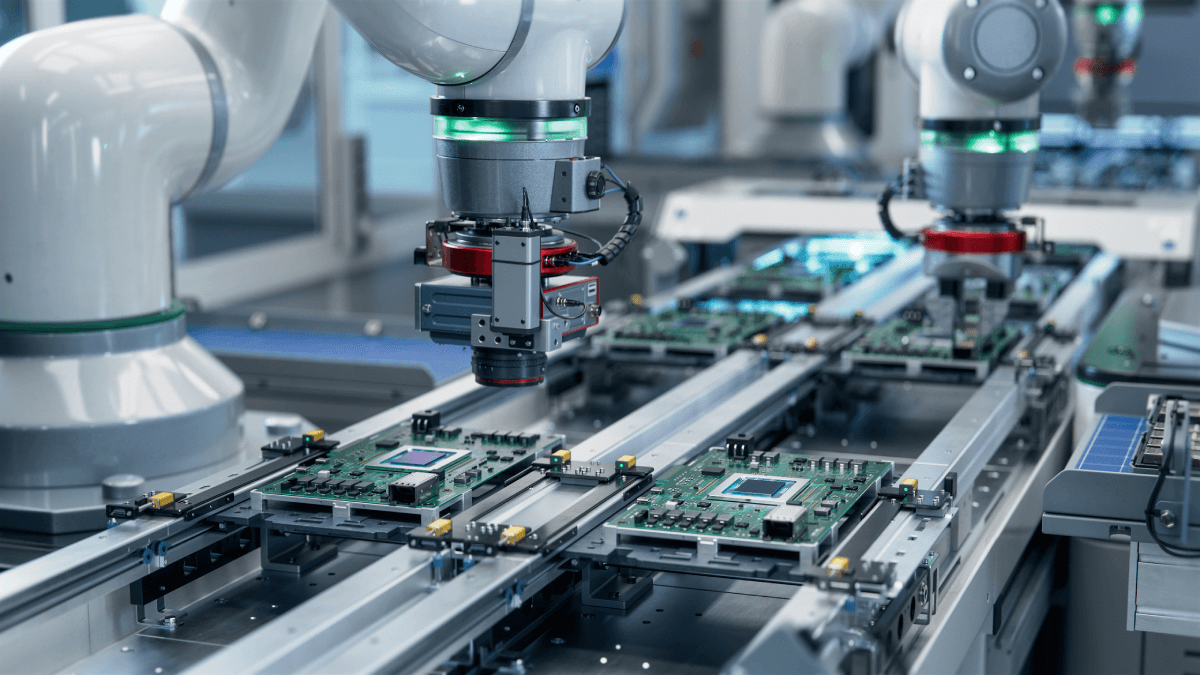
Automation Engineer
Skills Offered
Automating semiconductor production tools and processes using robotics/AI.
Education/Certifications Required
B.Tech/Diploma (Electrical/Electronics); Training in Robotics Process Automation (RPA).
Why Critical
Fabs are increasingly automated, requiring skilled experts to optimize automation workflows.